Event
- Title:
- Giovanni Vignale Seminar
- When:
- 23.06.2010 - 23.06.2010 15.00 h - 17.00 h
- Where:
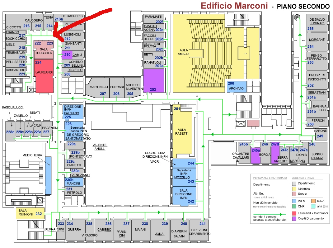
- Sala Touschek - Roma
- Category:
- Seminars
Description
Coulomb drag and spin Hall Drag: new coupling mechanisms for nanoelectronics
G. Vignale, University of Missouri-Columbia
G. Vignale, University of Missouri-Columbia
Double-layer structures consisting of two parallel quantum wells separated by a narrow potential barrier are an important class of nanoscale electronic devices. Each layer hosts a quasi-two dimensional electron gas and electrons interact across the barrier via the Coulomb interaction. When an electric current is driven in
one of the layers the Coulomb interaction causes a charge accumulation in the other layer. This phenomenon, known as Coulomb drag, is of fundamental interest as a probe of electron correlations and provides a new coupling mechanism between spatially separated elements of nano-electronic circuits, alternative to the conventional inductive and capacitive couplings. A second e ect of great interest is the Spin Hall E ect, i.e. the generation of spin accumulation by an electric current. This is due to spin-orbit interactions and has recently received great attention not only because of its theoretical subtlety but also for its usefulness as a source of spin-polarized currents. In this talk I review our current understanding of these two e ects and I describe a third one, which arises from the combination of spin Hall e ect and Coulomb drag. I call it Spin Hall Drag. The e ect consists in the generation of transversal spin accumulation in one layer by an electric
current in the other layer. Microscopic calculations indicate that the induced spin accumulation, although considerably smaller than the one observed in the ordinary spin Hall e ect, is large enough to be detected in optical rotation experiments.
Venue
- Venue:
- Sala Touschek - Website
- Street:
- Piazzale Aldo Moro, 2
- ZIP:
- 00185
- City:
- Roma
- State:
- Italy
- Country:
-

Description
Università La Sapienza. Edificio Marconi, 2nd floor
EventList powered by schlu.net